- 1. Clay PCB tutorial enables prototypes in 1-2 hours vs. 7-14 days for traditional boards.
- 2. Drops costs to pennies per unit from $5+ USD minimum runs (JLCPCB, 2024).
- 3. Perfect for startups amid Fear & Greed at 33 and BTC at $78,247 USD (CoinMarketCap).
Hardware startups use this Clay PCB tutorial to build custom printed circuit boards with conductive clay in hours. Bitcoin rallied to $78,247 USD (CoinMarketCap, Oct. 10, 2024) as Crypto Fear & Greed Index sits at 33 (Alternative.me, Oct. 10, 2024).
Ethereum trades at $2,367.73 USD, up 2.5% in 24 hours (CoinMarketCap, Oct. 10, 2024). XRP reaches $1.43 USD, up 0.8%. BNB climbs to $635.90 USD, up 1.1%. Lean teams bypass $500 minimum orders from JLCPCB.
Clay PCB Basics and Mechanics
Clay PCBs create traces from conductive clay on paper or foam substrates. Graphite powder delivers 1-10 ohms per cm resistivity for low-power circuits (Squishy Circuits, 2024).
Sculpt paths, insert components, and test with a multimeter. Air-dry or bake clay for durability. SparkFun offers conductive clay kits at $15 USD each (SparkFun, Oct. 2024). Embed LEDs, resistors, or ESP32 modules without CAD software.
This method suits crypto hardware prototypes like wallets or sensors, aligning with DeFi growth.
Why Startups Adopt Clay PCBs Now
VC funding for hardware startups fell 25% year-over-year to $1.8 billion USD in Q3 2024 (Crunchbase, Oct. 2024). Cautious markets with Fear & Greed at 33 demand rapid prototypes (Alternative.me, Oct. 10, 2024).
Bitcoin gained 1.2% to $78,247 USD (CoinMarketCap, Oct. 10, 2024). Traditional PCBs take 7-14 days and cost $5+ USD per unit (JLCPCB pricing, 2024).
Clay costs pennies and requires basic skills. Ethereum's 2.5% rise boosts DeFi hardware demand (CoinMarketCap, Oct. 10, 2024).
- Aspect: Time · Traditional PCB: 7-14 days · Clay PCB: 1-2 hours
- Aspect: Skill · Traditional PCB: Advanced CAD · Clay PCB: Beginner
- Aspect: Flexibility · Traditional PCB: Rigid · Clay PCB: Sculptable
- Aspect: Cost · Traditional PCB: $5+ USD min · Clay PCB: Pennies
Data from JLCPCB (2024) and Squishy Circuits (2024). Global PCB market reached $84 billion USD in 2023, projected to grow to $91.6 billion USD by 2028 at 4.5% CAGR (Statista, 2024).
Clay PCBs enable startups to capture market share amid crypto rallies.
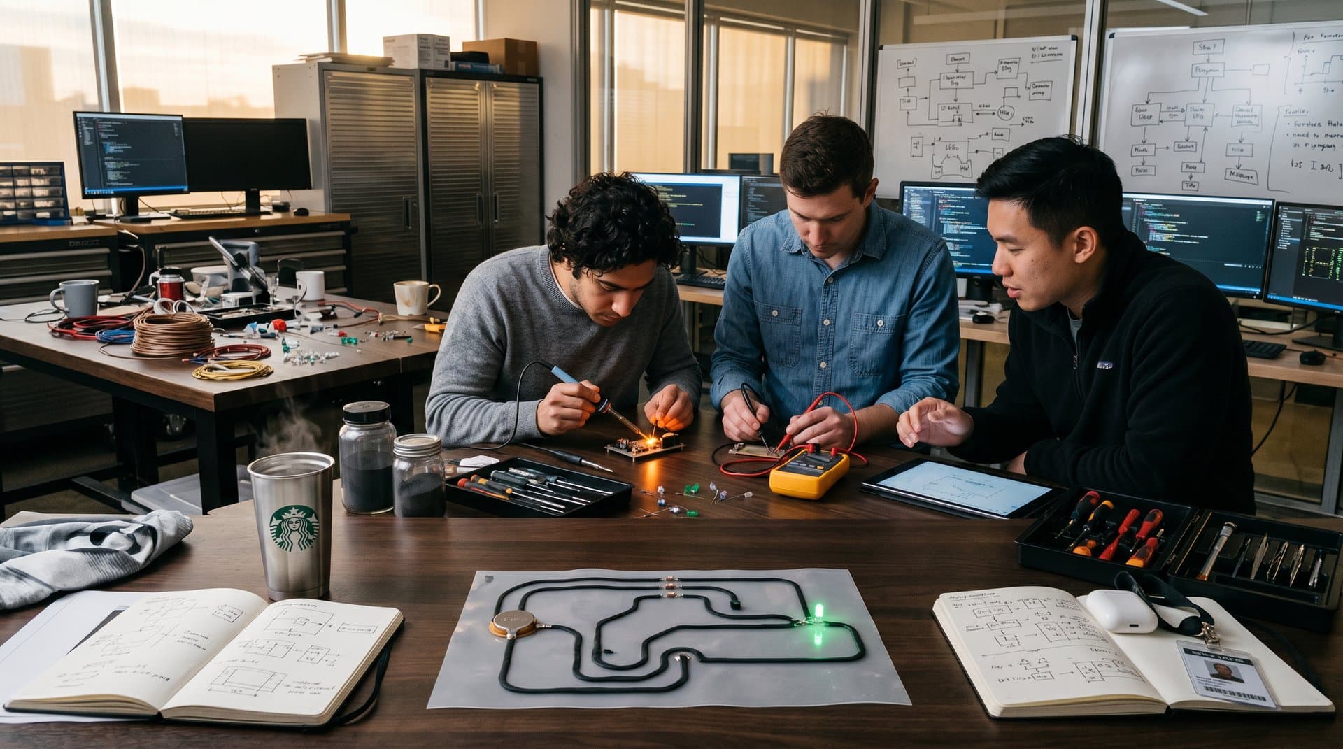
6-Step Clay PCB Tutorial
Step 1: Gather Materials
Collect non-toxic clay, graphite powder, multimeter, LEDs, coin cell batteries (CR2032), resistors (220-330 ohms), and cardstock. Bare Conductive's guide inspires mixes for reliable conductivity (Bare Conductive, 2024).
Prepare gloves and a clean workspace to avoid contamination.
Step 2: Mix Conductive Clay
Combine equal parts clay and graphite powder. Knead until uniform gray color forms. Test resistivity with multimeter—aim for under 20 ohms per cm. Add drops of water if too stiff. Store in airtight container.
Mixture lasts weeks, enabling multiple prototypes.
Step 3: Design Simple Circuit
Sketch a series circuit on paper: positive battery terminal to 220-ohm resistor, then LED anode, cathode to negative terminal. Keep traces 5 mm apart to prevent shorts. Pencil lines act as insulators.
Start with low-voltage (3V) for safety.
Step 4: Sculpt Traces on Substrate
Roll clay into 2-3 mm diameter snakes. Press firmly onto cardstock, forming 1-2 mm thick traces. Embed component leads directly into clay. Smooth edges to minimize resistance hotspots.
Ensure secure connections for reliable testing.
Step 5: Test and Debug Circuit
Connect coin battery. Use multimeter to verify continuity (under 50 ohms total). Power on—LED should illuminate steadily. Adjust clay thickness if dim. Adafruit's proto-snap methods add snap connectors for reusability (Adafruit, 2024).
Iterate quickly for optimal performance.
Step 6: Harden and Seal Board
Air-dry 24 hours or bake at 100°C for 30 minutes in oven. Apply clear varnish or acrylic sealant for protection. Transition proven designs to FR4 PCBs for production.
Scale prototypes to investor demos.
Clay Prototypes Boost Startup Funding Odds
Tangible clay demos impress VCs during pitches. XRP at $1.43 USD fuels blockchain hardware (CoinMarketCap, Oct. 10, 2024). USDT stable at $1.00 USD supports treasury planning.
Y Combinator emphasizes quick MVPs; clay delivers validation under $1 USD (Y Combinator guidelines, 2024). Hardware startups with prototypes raise 30% more funding (Crunchbase, 2024 analysis).
Clay PCB Future in Crypto Hardware
Silver-based inks and 3D-printed clay evolve the tech. Bitcoin stability at $78,247 USD accelerates secure wallet prototypes (CoinMarketCap, Oct. 10, 2024).
Fear & Greed at 33 tests resilience (Alternative.me, Oct. 10, 2024). This Clay PCB tutorial equips founders for hardware booms in volatile markets.
Frequently Asked Questions
What is a Clay PCB tutorial?
Clay PCB tutorial teaches sculpting conductive traces with clay and graphite for custom circuits. Skips etching for instant low-power prototypes using Arduino parts.
How to build Clay PCB projects?
Mix clay with graphite, sculpt traces, embed components. Test conductivity under 20 ohms. Air-dry for durable boards.
Why use Clay PCB tutorial for startups?
Cuts time to 1-2 hours vs. weeks. Saves costs amid BTC at $78,247 USD. Builds investor-ready MVPs fast.
Does Clay PCB replace etched boards?
Suits ideation with flexibility. Transition to FR4 after validation. Enhances with Bare Conductive materials.